Index
FileFile history
File usage
Global file usage
800 × 427 pixels
320 × 171 pixels
640 × 341 pixels
1,024 × 546 pixels
1,280 × 683 pixels
3,000 × 1,600 pixels
Original file
Wikimedia Commons
description page there
You can help
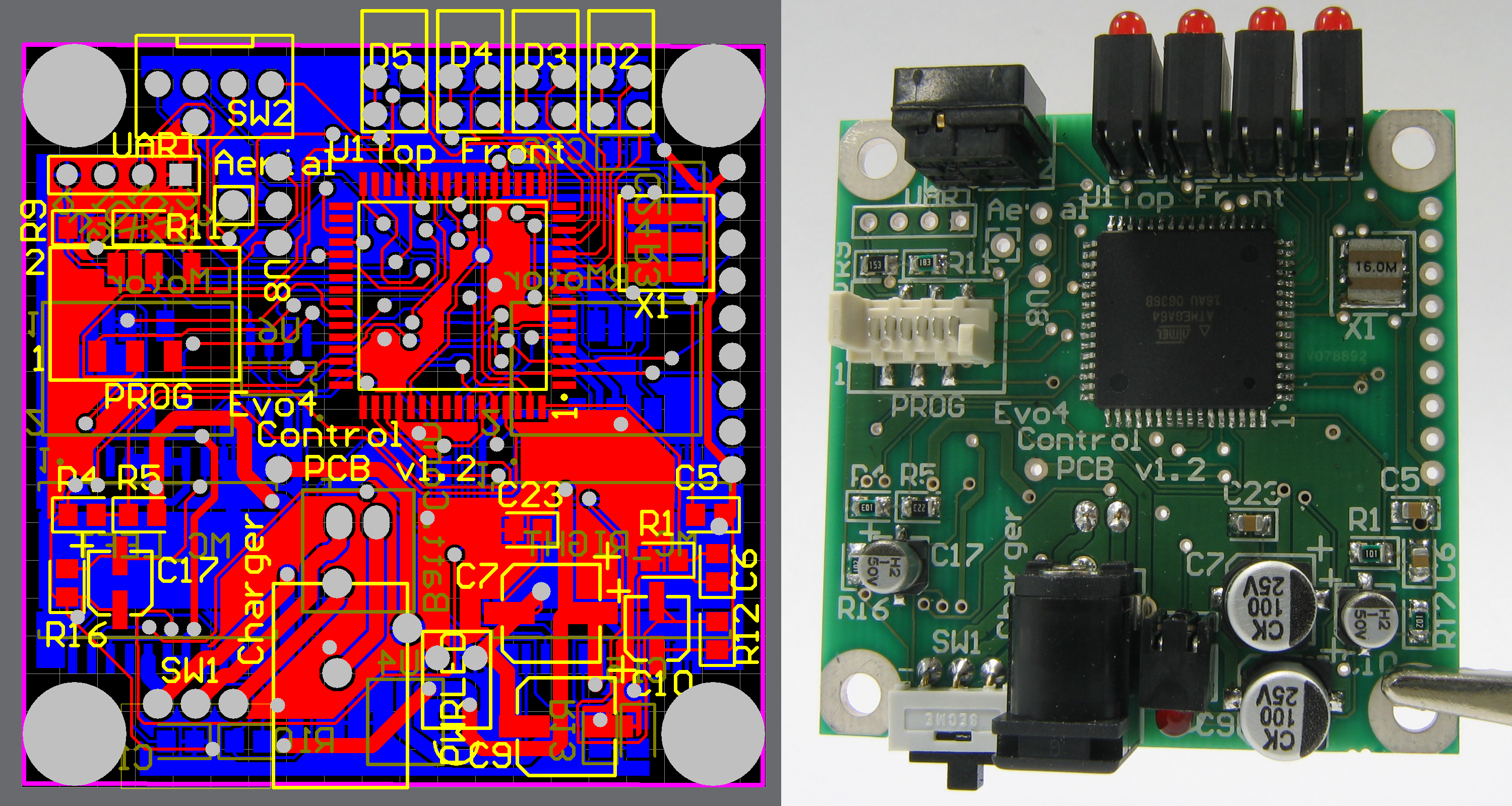
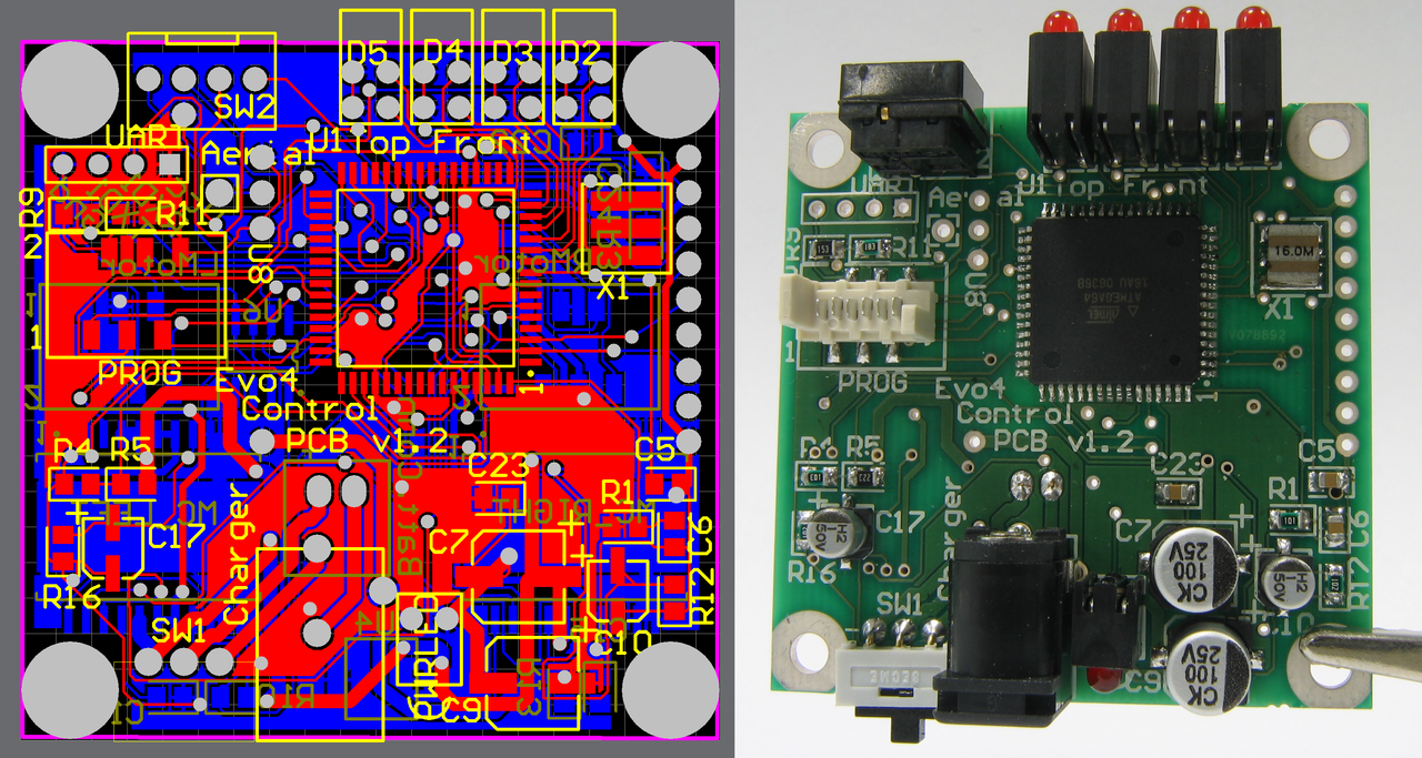
printed circuit board
circuito stampato
User:Mike1024
Mike1024
Reusing this file
public domain
depicts<\/a>"}},"text\/plain":{"en":{"":"depicts"}}},"{\"value\":{\"entity-type\":\"item\",\"numeric-id\":173350,\"id\":\"Q173350\"},\"type\":\"wikibase-entityid\"}":{"text\/html":{"en":{"P180":"printed circuit board<\/a>"}},"text\/plain":{"en":{"P180":"printed circuit board"}}}}">
In dieser Datei abgebildete Objekte
depicts
printed circuit board
copyright status<\/a>"}},"text\/plain":{"en":{"":"copyright status"}}},"{\"value\":{\"entity-type\":\"item\",\"numeric-id\":88088423,\"id\":\"Q88088423\"},\"type\":\"wikibase-entityid\"}":{"text\/html":{"en":{"P6216":"copyrighted, dedicated to the public domain by copyright holder<\/a>"}},"text\/plain":{"en":{"P6216":"copyrighted, dedicated to the public domain by copyright holder"}}},"{\"value\":{\"entity-type\":\"item\",\"numeric-id\":50423863,\"id\":\"Q50423863\"},\"type\":\"wikibase-entityid\"}":{"text\/html":{"en":{"P6216":"copyrighted<\/a>"}},"text\/plain":{"en":{"P6216":"copyrighted"}}}}">copyright status
copyrighted, dedicated to the public domain by copyright holder
copyrighted
copyright license<\/a>"}},"text\/plain":{"en":{"":"copyright license"}}},"{\"value\":{\"entity-type\":\"item\",\"numeric-id\":98592850,\"id\":\"Q98592850\"},\"type\":\"wikibase-entityid\"}":{"text\/html":{"en":{"P275":"released into the public domain by the copyright holder<\/a>"}},"text\/plain":{"en":{"P275":"released into the public domain by the copyright holder"}}}}">copyright license
released into the public domain by the copyright holder
inception<\/a>"}},"text\/plain":{"en":{"":"inception"}}},"{\"value\":{\"time\":\"+2007-02-02T00:00:00Z\",\"timezone\":0,\"before\":0,\"after\":0,\"precision\":11,\"calendarmodel\":\"http:\\\/\\\/www.wikidata.org\\\/entity\\\/Q1985727\"},\"type\":\"time\"}":{"text\/html":{"en":{"P571":"2 February 2007"}},"text\/plain":{"en":{"P571":"2 February 2007"}}}}">
Text is available under the Creative Commons Attribution-ShareAlike License. Additional terms may apply.
↑
copyright status
copyrighted, dedicated to the public domain by copyright holder
copyrighted
copyright license<\/a>"}},"text\/plain":{"en":{"":"copyright license"}}},"{\"value\":{\"entity-type\":\"item\",\"numeric-id\":98592850,\"id\":\"Q98592850\"},\"type\":\"wikibase-entityid\"}":{"text\/html":{"en":{"P275":"released into the public domain by the copyright holder<\/a>"}},"text\/plain":{"en":{"P275":"released into the public domain by the copyright holder"}}}}">copyright license
released into the public domain by the copyright holder
inception<\/a>"}},"text\/plain":{"en":{"":"inception"}}},"{\"value\":{\"time\":\"+2007-02-02T00:00:00Z\",\"timezone\":0,\"before\":0,\"after\":0,\"precision\":11,\"calendarmodel\":\"http:\\\/\\\/www.wikidata.org\\\/entity\\\/Q1985727\"},\"type\":\"time\"}":{"text\/html":{"en":{"P571":"2 February 2007"}},"text\/plain":{"en":{"P571":"2 February 2007"}}}}">
Text is available under the Creative Commons Attribution-ShareAlike License. Additional terms may apply.
↑
copyright license
released into the public domain by the copyright holder
inception<\/a>"}},"text\/plain":{"en":{"":"inception"}}},"{\"value\":{\"time\":\"+2007-02-02T00:00:00Z\",\"timezone\":0,\"before\":0,\"after\":0,\"precision\":11,\"calendarmodel\":\"http:\\\/\\\/www.wikidata.org\\\/entity\\\/Q1985727\"},\"type\":\"time\"}":{"text\/html":{"en":{"P571":"2 February 2007"}},"text\/plain":{"en":{"P571":"2 February 2007"}}}}">
Text is available under the Creative Commons Attribution-ShareAlike License. Additional terms may apply.
↑
Text is available under the Creative Commons Attribution-ShareAlike License. Additional terms may apply.
↑